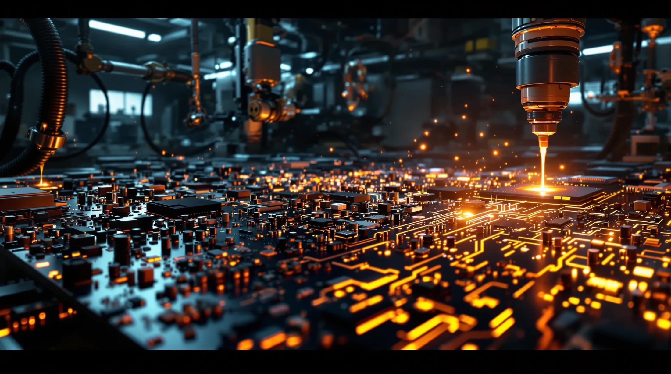
PCB Assembly: A Comprehensive Guide to Efficient Manufacturing
Discover the intricate world of PCB assembly, where precision engineering meets advanced manufacturing to create the electronic devices that power our modern world. Whether you’re an engineer, manufacturer, or electronics enthusiast, understanding this critical process is essential for successful electronic product development.
Understanding PCB Assembly
PCB assembly transforms bare printed circuit boards into functional electronic devices through a sophisticated manufacturing process. This vital stage combines precision engineering, specialized equipment, and stringent quality control measures to ensure reliable performance in countless everyday devices.
Modern PCB assembly encompasses various soldering techniques, each carefully selected based on component requirements and production volumes. From simple single-layer boards to complex multi-layer designs, standardized assembly procedures ensure consistent quality and reliability.
The Basics of PCB Assembly
The assembly process centers on attaching electronic components to a fabricated circuit board, creating a functional electronic circuit. Starting with a bare PCB designed with specific pathways, pads, and holes, components are strategically positioned according to precise specifications.
| Assembly Method | Description | Best Use Case |
|---|---|---|
| Surface Mount Technology (SMT) | Components mounted directly on PCB surface | High-density, compact designs |
| Through-Hole Technology (THT) | Components inserted through pre-drilled holes | High-reliability applications |
Key Steps in the PCB Assembly Process
- Design for Manufacture (DFM) verification
- Solder paste application through screen printing
- Component placement (manual or automated)
- Reflow soldering process
- Comprehensive testing and inspection
- Quality assurance and final treatments
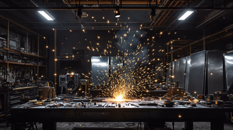
Soldering Techniques in PCB Assembly
Soldering represents the foundation of PCB assembly, creating reliable electrical connections through molten metal alloys. The quality of these connections directly influences device performance and longevity, making proper technique selection crucial for successful manufacturing.
Through-Hole vs. Surface Mount Technology
These two primary methodologies serve different purposes in modern electronics manufacturing. Through-Hole Technology provides robust mechanical connections ideal for harsh environments, while Surface Mount Technology enables higher component density and efficient automation.
Advantages of Automated Assembly Machines
- Placement speeds up to 60,000 components per hour
- Precision accuracy of ±0.03mm
- Reduced labor costs and material waste
- Comprehensive process data collection
- Integration of multiple assembly functions
- Consistent quality in high-volume production
Ensuring Quality Control in PCB Assembly
Quality control is a critical component of PCB assembly that directly impacts the reliability and performance of electronic devices. Professional PCB manufacturers integrate quality assurance throughout the entire assembly process, rather than treating it as a final checkpoint. This comprehensive approach enables early detection and resolution of potential issues, minimizing defects in finished products.
Manufacturers like Colorado PCB Assembly implement collaborative quality control systems where team members share unified standards and work closely on each build. This collective approach ensures consistency across production runs and establishes reliable foundations that customers depend on.
- Verification of design specifications
- Compliance with ROHS-Lead Free requirements
- Adherence to UL certifications
- Continuous monitoring throughout production
- Team-based quality responsibility
Common Inspection Methods
| Inspection Method | Application | Capabilities |
|---|---|---|
| Automated Optical Inspection (AOI) | Visual examination | Component placement, solder joint quality |
| Electronic Testing (E-Test) | Electrical verification | Circuit functionality, connections |
| X-Ray Inspection | Hidden features | BGA connections, internal layers |
Importance of Quality Control
Quality control directly correlates with the functionality, reliability, and lifespan of electronic products. Defective assemblies can result in field failures, product recalls, and significant financial losses. Beyond immediate costs, quality issues can damage brand reputation and customer confidence.
- Essential for complex PCB designs with smaller components
- Critical for medical devices and aerospace applications
- Ensures consistent performance under operating conditions
- Reduces warranty claims and strengthens customer relationships
- Prevents potential safety hazards in critical applications
Materials and Environmental Considerations
Material selection in PCB assembly significantly influences performance, reliability, durability, and environmental impact. Each material choice represents a careful balance between technical requirements, cost considerations, and environmental responsibility, all while adhering to global regulations.
Choosing the Right Materials
- Substrate materials (FR-4, polyimide, ceramics) based on application needs
- Copper foil thickness selection for current capacity
- Solder paste types (Type 3 or Type 4) for fine-pitch components
- Specialized alloys for high-reliability applications
- Flux compatibility with cleaning requirements
Environmental considerations have become paramount in PCB manufacturing, driven by regulations like the EU’s RoHS Directive. These developments have transformed industry practices, particularly in soldering materials and processes, promoting sustainable approaches without compromising product quality or reliability.
Environmental Impact and Lead-Free Soldering
The transition to lead-free soldering marks a pivotal environmental advancement in PCB assembly. Modern manufacturers have largely replaced traditional tin-lead solders (Sn63/Pb37) with environmentally conscious alternatives like SAC305 (96.5% tin, 3% silver, 0.5% copper). This shift significantly reduces toxic lead contamination in landfills and groundwater from electronic waste.
| Solder Type | Composition | Melting Temperature |
|---|---|---|
| Traditional Tin-Lead | Sn63/Pb37 | 183°C |
| Lead-Free SAC305 | 96.5% Sn, 3% Ag, 0.5% Cu | 217-220°C |
Environmental considerations extend beyond solder composition in modern PCB assembly. Forward-thinking manufacturers implement comprehensive environmental management systems that address multiple aspects of production:
- Energy-efficient reflow ovens for reduced power consumption
- Water-based cleaning systems replacing solvent-based alternatives
- Waste reduction programs for flux residues and cleaning agents
- Water usage optimization in cleaning processes
- Systematic tracking of environmental impacts
Prototyping and Collaboration in PCB Assembly
PCB prototyping faces significant financial challenges, with most assembly companies requiring minimum orders of $500 or more. This cost barrier often impacts the iterative design phase, where frequent modifications are necessary. However, effective collaboration between design teams and assembly partners can substantially improve project outcomes and reduce time-to-market.
The Role of Prototyping
Prototyping serves as an essential validation step between theoretical design and mass production, particularly crucial for complex designs involving high-frequency components or mixed-signal applications. This phase enables engineers to:
- Detect design flaws before mass production
- Verify component compatibility
- Assess performance limitations
- Test systems under actual operating conditions
- Optimize designs for manufacturing efficiency
Enhancing Efficiency Through Collaboration
Early collaboration between design teams and assembly partners can reduce production costs by 15-30% through optimized board layouts and manufacturing processes. Advanced kitting processes exemplify this collaborative approach, organizing components before assembly to reduce production time and minimize errors.
- Consistent personnel throughout project phases
- Specialized knowledge retention about component placement
- Early identification of manufacturing challenges
- Streamlined workflow through organized kitting
- Improved yield rates through design optimization