PCB Manufacturing: A Comprehensive Guide to Processes and Techniques
Discover the intricate world of Printed Circuit Board (PCB) manufacturing, where design innovation meets precision engineering. Whether you’re an electronics enthusiast, engineer, or industry professional, understanding this fundamental process is crucial for creating reliable electronic devices.
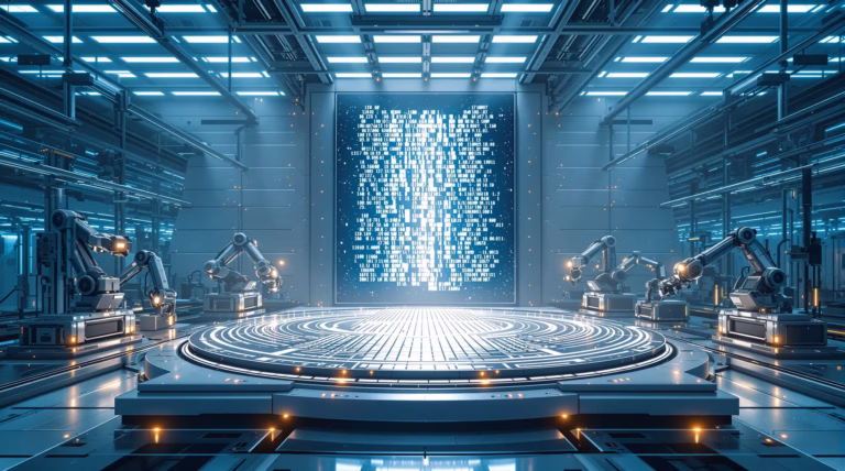
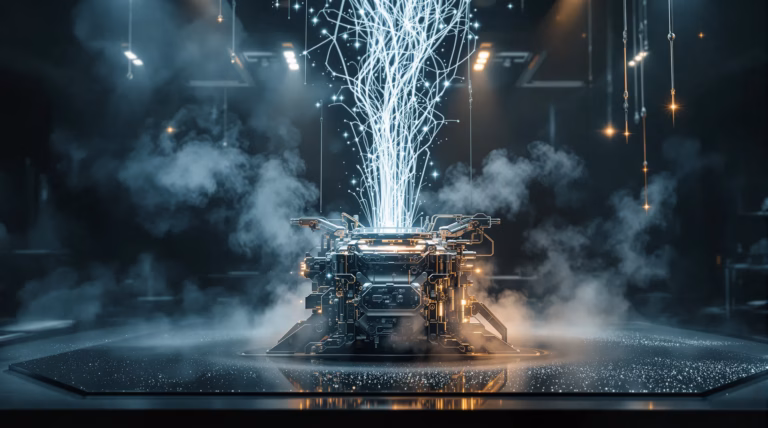
Printed Circuit Board (PCB) manufacturing forms the foundation of modern electronics, enabling the creation of sophisticated electronic circuits that power everything from smartphones to aerospace systems. The process transforms design files into functional circuit boards through a series of precise manufacturing steps.
The manufacturing journey encompasses several critical phases:
- Design creation using specialized CAD software
- Conversion to Gerber files for fabrication
- Inner layer imaging and etching
- Component placement and assembly
- Quality control and testing
Designing the PCB Layout
PCB layout design requires careful balance between electrical performance and manufacturing constraints. Professional designers adhere to established design rules that govern:
- Trace width and spacing requirements
- Pad dimensions and tolerances
- Component placement optimization
- Signal integrity considerations
- Electromagnetic interference prevention
Using CAD Software for PCB Design
Modern PCB design relies on sophisticated CAD software platforms that offer comprehensive design environments. These tools provide essential features for professional PCB creation:
| Software | Key Features |
|---|---|
| Altium Designer | Advanced routing, 3D visualization, comprehensive DRC |
| Eagle | Cost-effective, extensive component libraries |
| KiCad | Open-source, growing community support |
| OrCAD | Robust simulation capabilities, enterprise integration |
| Siemens Xpedition | High-end features, advanced thermal modeling |
Creating and Using Gerber Files
Gerber files serve as the universal language between designers and manufacturers, containing detailed information for fabrication. A complete Gerber package includes:
- Copper layer specifications
- Solder mask definitions
- Silkscreen markings
- Drill locations and specifications
- Board outline information
- Stack-up documentation
Materials Used in PCB Manufacturing
PCB manufacturing relies on three fundamental components that determine board performance and reliability:
- Conductive materials – primarily copper for electrical pathways
- Insulating substrates – typically fiberglass-based materials
- Bonding agents – epoxy resins for layer adhesion
- Specialized materials for specific applications (PTFE, Rogers)
- Thermal management materials (aluminum-based substrates)
Common Materials: Copper, Fiberglass, and Epoxy
Copper serves as the fundamental material in PCB manufacturing, distinguished by its superior electrical conductivity, solderability, and cost-effectiveness. Standard PCBs typically utilize 1 oz/ft² copper foil, while heavy copper PCBs employ thicker layers (3-20 oz/ft²) for high-current applications requiring enhanced thermal management. The copper quality and surface treatment directly influence signal integrity and board longevity.
| Copper Weight | Application |
|---|---|
| 1 oz/ft² | Standard applications |
| 3-20 oz/ft² | High-current, thermal-critical applications |
The substrate structure combines fiberglass (primarily FR4) with epoxy resin to create a robust foundation. This composite delivers:
- Mechanical support and stability
- Electrical isolation between layers
- Tensile strength from fiberglass weave
- Moisture resistance through epoxy impregnation
- Thermal cycling endurance
Environmental Considerations in Material Selection
Modern PCB manufacturing increasingly focuses on environmental responsibility through careful material selection and process optimization. Manufacturers now implement comprehensive environmental strategies that include:
- Adoption of halogen-free laminates
- Implementation of lead-free surface finishes
- Use of water-based chemicals
- Reduction of VOC-emitting solvents
- Elimination of harmful brominated flame retardants
Material recycling has become integral to sustainable PCB manufacturing. Advanced recycling processes enable the recovery of valuable materials:
- Copper extraction from circuit traces
- Precious metal recovery (gold, silver, palladium)
- Closed-loop chemical processing systems
- Waste reduction strategies
- Safe disposal of hazardous substances
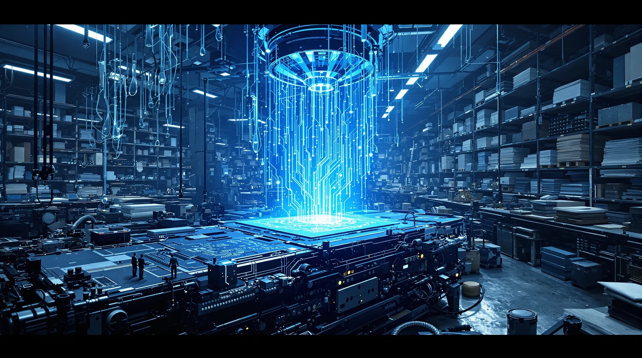
The PCB Fabrication Process
PCB fabrication follows a precise sequence of operations, transforming raw materials into functional circuit boards. The process maintains strict environmental controls throughout, as factors like temperature, humidity, and contamination significantly impact product quality.
- Inner layer imaging and pattern transfer
- Copper etching for circuit formation
- Multi-layer lamination processes
- Precision drilling operations
- Through-hole plating procedures
- Outer layer circuit definition
- Solder mask application
- Surface finish treatment
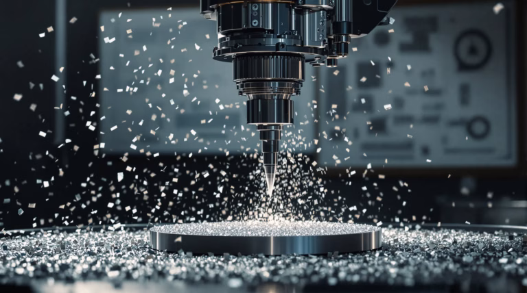
Etching and Drilling Techniques
PCB etching employs two primary methods for circuit pattern creation:
- Chemical etching using alkaline or acidic solutions
- Plasma etching for fine-line precision
- Controlled solution concentration and temperature
- Precise exposure timing
- Clean trace geometry maintenance
Drilling operations utilize advanced CNC technology and specialized equipment:
- Hole diameters ranging from 0.1mm to 6.5mm
- Optical alignment systems for precise positioning
- Laser drilling for microvias (sub-0.1mm)
- Sophisticated dust extraction systems
- Entry/exit material protection
Plating and Solder Mask Application
Plating processes establish electrically conductive pathways through PCB holes while enhancing surface copper durability and solderability. The process begins with electroless copper deposition, creating a thin conductive layer on non-metallic surfaces. This initial layer enables subsequent electroplating, where panels are submerged in copper sulfate solutions while electrical current deposits additional copper onto conductive surfaces.
- Electroless copper deposition for initial conductivity
- Copper electroplating for enhanced conductivity
- Specialized metallic layers (nickel, gold, silver, tin)
- Oxidation prevention treatments
- Solderability enhancement processes
Solder mask application involves a protective polymer coating that shields copper traces while maintaining exposed component connection pads. Modern facilities utilize liquid photoimageable solder masks through:
- Screen printing or spray coating application
- UV exposure through photomasks
- Selective polymer curing
- Thermal curing for final hardness
- Precise thickness control (10-25 microns)
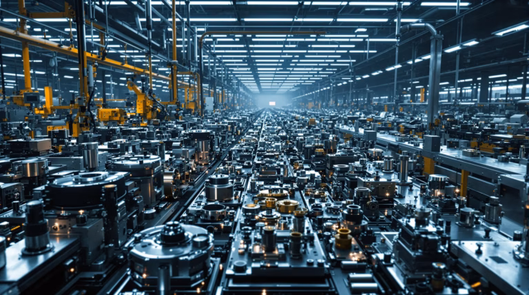
PCB Assembly and Testing
PCB assembly transforms bare circuit boards into functional electronic systems through precise component placement and securing operations. The process employs both Surface Mount Technology (SMT) and Through-Hole Technology (THT), often combining both approaches for optimal performance. Rigorous testing protocols verify electrical functionality, identify defects, and ensure compliance with design specifications.
Automated Assembly with Pick and Place Machines
Pick and place machines form the backbone of modern automated PCB assembly, utilizing vacuum nozzles on high-speed positioning heads for precise component placement. Advanced systems like the Yamaha YSM 20 achieve placement rates of thousands of components per hour with micrometer-level accuracy.
- Optical recognition for component verification
- Polarity and positioning confirmation
- Handling of diverse component packages (01005 to large ICs)
- Multiple machine configuration for optimized production
- Error reduction through automation
Testing Methods: E-Test, Flying Probe, and Bed of Nails
| Testing Method | Key Features |
|---|---|
| E-Testing | Basic continuity, shorts, and opens verification |
| Flying Probe | Flexible testing without custom fixtures, ideal for prototypes |
| Bed of Nails | High-volume testing with custom fixtures for rapid verification |
Additional verification methods include In-Circuit Testing (ICT), Automated Optical Inspection (AOI), and comprehensive Functional Testing, creating a multi-layered approach to quality assurance. This combination ensures product reliability and minimizes field failures through early defect detection.
Quality Control in PCB Manufacturing
Quality control forms the backbone of PCB manufacturing, ensuring reliability and optimal performance in electronic products. The comprehensive QA/QC protocols integrate multiple inspection stages throughout the fabrication and assembly workflow, validating both physical construction and electrical performance standards.
- Design Rule Checks (DRC) during pre-production
- Automated Optical Inspection (AOI) for surface defects
- Electronic Testing (E-Test) for circuit validation
- X-Ray Inspection for internal structure examination
- Impedance testing for signal integrity
- RoHS and lead-free compliance verification
- UL certification for safety requirements
Ensuring Reliability and Performance
Advanced manufacturers implement a multi-tiered approach to reliability, starting with material verification and extending through final functionality testing. For mission-critical applications, comprehensive evaluations include:
- Thermal cycling assessments
- Humidity resistance testing
- Vibration analysis
- Performance validation across operating conditions
- Impedance control measurements
- Internal structure examination via X-ray systems
Advanced PCB Technologies and Trends
The PCB manufacturing industry continues evolving through miniaturization demands and emerging technology integration. Modern facilities utilize state-of-the-art equipment like the Dage XD6600 X-ray inspection system, while rapid prototyping services deliver boards within 24 hours for accelerated development cycles.
High-Density Interconnect (HDI) PCBs
| Feature | Benefit |
|---|---|
| Microvias (<0.15mm) | Efficient space utilization and higher connection density |
| Finer lines and spaces | Enhanced circuit density per unit area |
| Shorter connection paths | Improved signal integrity and reduced propagation delays |
| Optimized ground planes | Superior EMI performance |
Flexible PCBs and IoT Integration
Flexible printed circuits utilize polyimide-based materials for bendable, foldable designs that conform to three-dimensional shapes. These boards enable innovative solutions in space-constrained applications while offering:
- Reduced weight compared to rigid boards
- Enhanced durability against vibration
- Improved thermal cycling resistance
- Direct antenna integration capabilities
- Seamless sensor embedding options
The convergence of flexible PCB technology with IoT capabilities has accelerated smart device development across medical, automotive, and consumer electronics sectors, driving continuous innovation in manufacturing processes and design approaches.
Conclusion
PCB manufacturing has evolved into a sophisticated, multi-stage process that combines precision engineering with advanced automation. From initial design creation to final quality assurance, each step in the manufacturing workflow requires meticulous attention to detail to ensure reliable, high-performance circuit boards. The industry continues to push boundaries with increasingly complex designs, finer tolerances, and enhanced capabilities to meet the demands of modern electronics.
Future Outlook and Industry Trends
- Expanding applications in automotive electronics and 5G infrastructure
- Integration with medical devices and IoT systems
- Advanced technologies enabling higher component densities
- Improved signal integrity and thermal management solutions
- Enhanced focus on sustainable manufacturing practices
- Development of environmentally friendly materials
- Optimization of waste reduction processes
- Implementation of energy-efficient production methods
As electronic devices become more prevalent in every aspect of modern life, the PCB manufacturing sector will continue to adapt and innovate, providing the essential foundation for tomorrow’s technological advancements. The industry’s commitment to sustainability, coupled with advancing technological capabilities, positions PCB manufacturing at the forefront of electronic innovation.