Circuit Board Manufacturing: A Comprehensive Guide to the Process
Discover the intricate world of circuit board manufacturing, where precision engineering meets cutting-edge technology to create the foundation of modern electronics. From smartphones to aerospace systems, printed circuit boards (PCBs) are the essential components that power our digital world.
Understanding Circuit Board Manufacturing
Circuit board manufacturing is the foundational process that enables modern electronics to function. This complex production cycle transforms raw materials into sophisticated Printed Circuit Boards (PCBs) that serve as the backbone for virtually all electronic devices. The manufacturing process encompasses several crucial stages including design, fabrication, and assembly, each requiring precise execution to ensure functionality and reliability.
With advancements in technology, PCB manufacturing has evolved from simple single-layer boards to complex multi-layer structures capable of supporting intricate electronic systems. Contemporary manufacturing facilities operate 24/7 with teams of skilled professionals utilizing state-of-the-art equipment to meet growing demands for faster turnaround times, higher quality, and increasing miniaturization of electronic components.
What is Circuit Board Manufacturing?
Circuit board manufacturing is the process of creating printed circuit boards that connect electronic components through conductive pathways, traces, and pads etched from copper sheets laminated onto a non-conductive substrate. The process involves multiple specialized techniques:
- Surface Mount Technology (SMT) for component mounting
- Through-Hole Technology (THT) for secure connections
- Inner layer imaging and etching processes
- Photoresist stripping and outer layer imaging
- Precision drilling and plating operations
- Final assembly and quality control
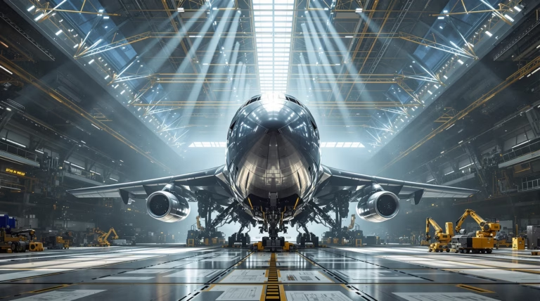
Importance of Circuit Boards in Modern Electronics
Circuit boards form the critical infrastructure of contemporary electronics, functioning as more than just component connectors—they are the nervous system that enables device functionality. Every electronic device, from smartphones and medical equipment to automotive systems and aerospace technology, relies on PCBs to establish electrical connections between components such as resistors, capacitors, and microprocessors.
| Application Area | PCB Contribution |
|---|---|
| Consumer Electronics | Enables compact design and efficient power distribution |
| Medical Devices | Provides reliable operation and precise signal processing |
| Automotive Systems | Supports advanced safety features and engine management |
| Aerospace Technology | Ensures durability and performance in extreme conditions |
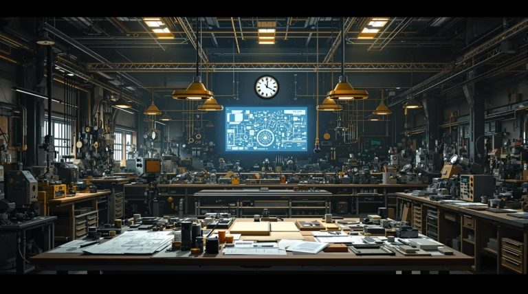
The PCB Design Process
The PCB design process forms the critical foundation of circuit board manufacturing, transforming conceptual electronic designs into manufacturable specifications. This multi-stage process begins with product concept development, followed by schematic entry where engineers define the electrical connections between components.
Key Considerations in PCB Design
Successful PCB design requires careful attention to numerous technical factors that influence both functionality and manufacturability. Essential design elements include:
- Component density optimization
- Signal integrity management
- Power distribution planning
- Thermal management strategies
- Electromagnetic compatibility considerations
- Layer count determination
- Material selection criteria
Software Tools for PCB Design
PCB design software serves as the primary instrument enabling engineers to create, simulate, and validate circuit designs before committing to production. Modern design platforms offer comprehensive capabilities for schematic capture, component library management, circuit simulation, layout design, autorouting, and design rule checking.
Advanced packages provide 3D visualization, signal integrity analysis, thermal simulation, and direct integration with manufacturing systems to streamline the transition from design to production. These sophisticated tools help ensure optimal design outcomes while minimizing production errors and reducing time-to-market.
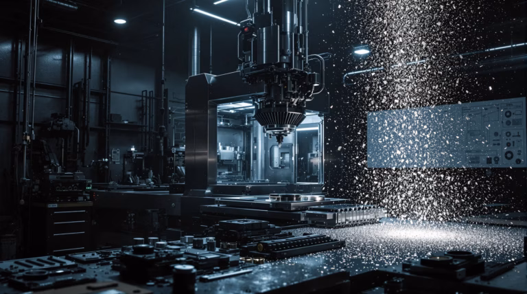
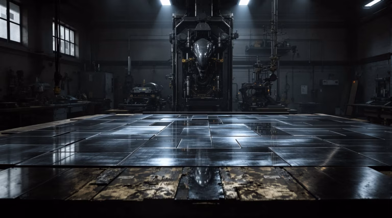
PCB Fabrication Techniques
PCB fabrication transforms circuit designs into physical hardware through a series of precise manufacturing steps. This complex process encompasses critical operations including etching, layering, drilling, and solder mask application to create intricate pathways for component interconnection. The precision of these techniques directly influences the reliability and performance of the final electronic product.
Modern fabrication facilities balance automated precision with skilled human oversight. Before production begins, specialists review designs for manufacturability issues, particularly in rapid prototyping environments. As electronics trend toward greater miniaturization and complexity, fabrication techniques have evolved to handle multi-layer structures, high-density interconnects, and specialized substrate materials.
Materials Used in PCB Fabrication
- FR4 – flame-resistant fiberglass-reinforced epoxy laminate offering excellent electrical insulation and mechanical stability
- Aluminum substrates – specialized material for enhanced thermal management
- Copper-core boards – designed for high power applications
- Rogers/PTFE-based substrates – optimized for radio frequency and microwave circuits
- Prepregs – pre-impregnated fiberglass sheets with partially cured resin
- Cores – fully cured fiberglass sheets with copper foil on both sides
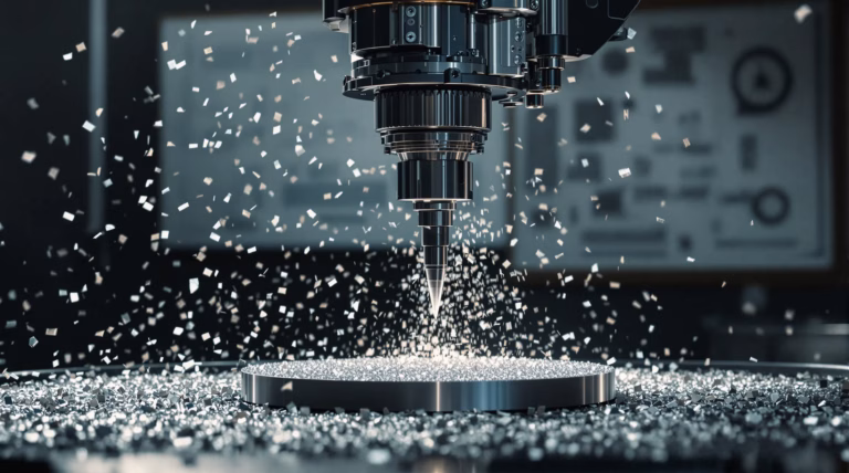
Common PCB Fabrication Methods
| Method | Description |
|---|---|
| Subtractive Manufacturing | Selective etching of copper-clad laminates using photoresist and chemical solutions |
| Additive Processing | Selective copper deposition on non-conductive substrates for high-precision applications |
| PCB Milling | CNC-based mechanical removal of copper from substrate |
| V-scoring | Creation of partial cuts in panels for efficient board separation |
| Backdrilling | Removal of excess copper from plated through-holes for improved signal integrity |
Printed Circuit Board Assembly
PCB assembly marks the transition from bare boards to functional electronic systems through component mounting and securing processes. This phase integrates advanced technologies with skilled manual techniques, depending on production requirements and design complexity.
Soldering Techniques in PCB Assembly
- Reflow Soldering – primary method for surface-mount components, involving solder paste application and controlled heating
- Wave Soldering – technique for through-hole components using waves of molten solder
- Manual Soldering – precision hand-soldering by skilled technicians for complex or low-volume production
Quality soldering requires careful attention to solder alloy selection, flux types, and maintaining clean work conditions. The integrity of these connections directly impacts electrical performance, long-term reliability, and resistance to environmental stresses.
Automated vs. Manual PCB Assembly
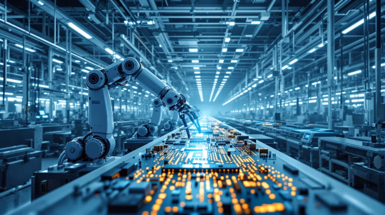
Automated assembly utilizes sophisticated pick-and-place machines capable of positioning thousands of components per hour with microscopic precision. These systems excel in high-volume production environments, offering consistent quality, reduced labor costs, and rapid throughput. Modern automated systems can handle components as small as 01005 (0.4mm × 0.2mm) and support mixed technology boards combining surface-mount and through-hole components.
- Automated Assembly Benefits – consistent quality, high-speed production, microscopic precision, reduced labor costs
- Manual Assembly Advantages – flexibility for prototypes, handling of unusual components, quick design adaptation
- Hybrid Approach Features – combines automation efficiency with human expertise, ideal for high-mix low-volume production
Quality Control in PCB Manufacturing
Quality control ensures every PCB meets stringent performance standards through comprehensive protocols implemented from design verification to final testing. These protocols identify and resolve potential issues affecting electrical performance, mechanical integrity, and long-term reliability.
Standards and Certifications in PCB Manufacturing
- RoHS Compliance – ensures boards are free from harmful materials like lead, mercury, and cadmium
- UL Certification – verifies PCBs meet safety standards for hazardous environments and high-power applications
- ISO 9001 – demonstrates consistent quality management systems
- IPC Standards – provides guidelines for design, manufacturing, and acceptance criteria
Testing Methods for PCBs
| Testing Method | Purpose |
|---|---|
| Automated Optical Inspection (AOI) | Detects visible defects using high-resolution cameras and pattern recognition |
| Automated X-ray Inspection (AXI) | Examines internal layers and hidden solder joints |
| In-Circuit Testing (ICT) | Checks individual components and connections using probe points |
| Flying Probe Testing | Fixture-less testing using mobile probes |
| Functional Testing | Simulates actual operating conditions for comprehensive verification |
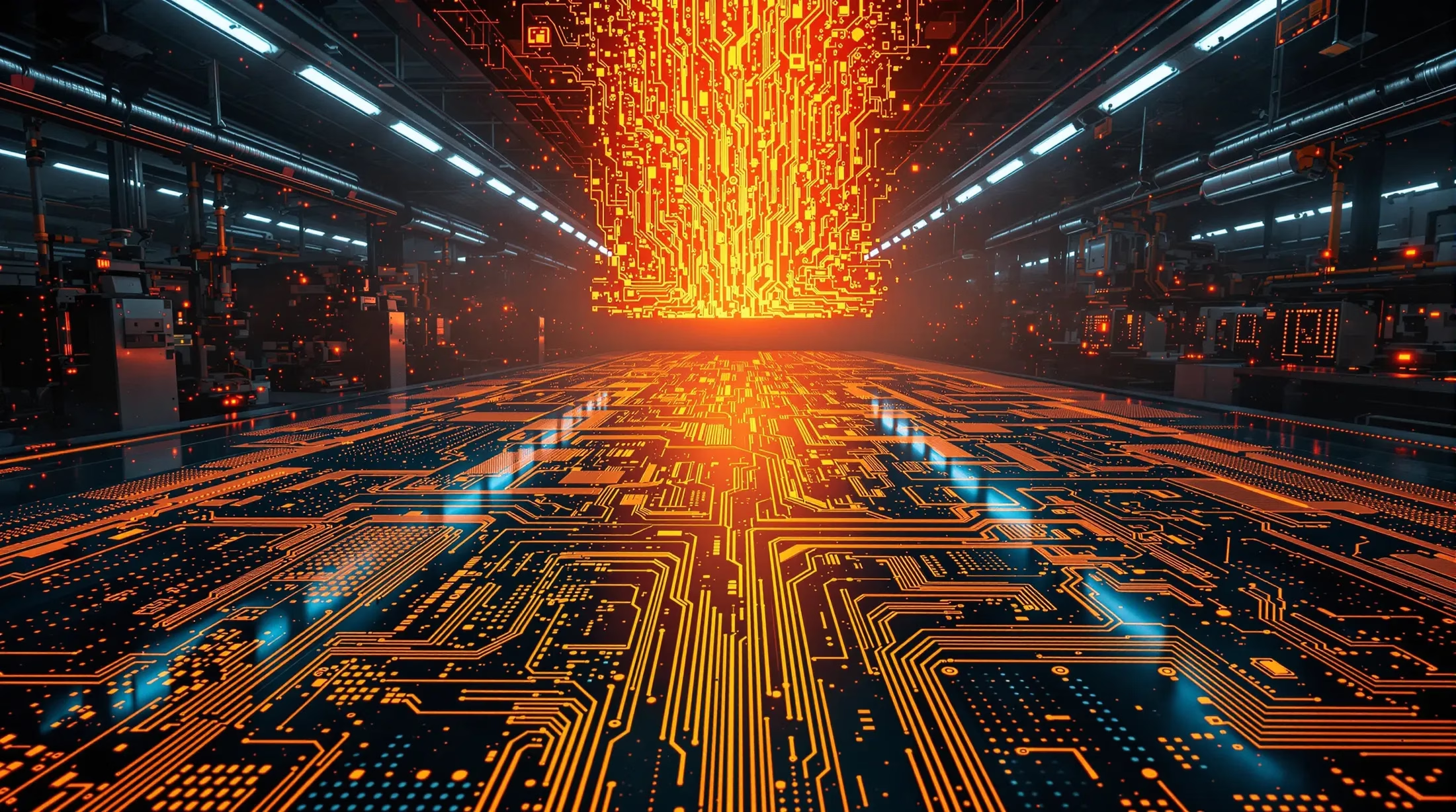
Future Trends in Circuit Board Manufacturing
The PCB manufacturing industry is experiencing significant transformation through technological advancements and market demands. Smart factory solutions incorporating artificial intelligence, machine learning, and advanced robotics are improving precision, reducing errors, and accelerating production timelines.
A significant industry shift has occurred with the democratization of PCB manufacturing services. Small businesses and hobbyists now have access to professional-grade PCB production at affordable prices, sometimes as low as $10 for small batches. This accessibility has enabled designers to focus on innovation while leveraging specialized manufacturers, particularly in Asia, for cost-effective production.
Innovations in PCB Technology
The evolution of PCB technology continues to accelerate, meeting the demands of increasingly complex electronic devices. Advanced multi-layer laminated structures have become standard, enabling higher component densities and improved performance in smaller form factors. High-density interconnect (HDI) technology, featuring laser-drilled microvias and finer line spacing, drives miniaturization essential for modern smartphones and wearable devices.
- Quick-turn Fabrication – streamlined processes reducing production times from weeks to hours
- Enhanced Design Verification – simulation tools for electrical, thermal, and mechanical performance
- Flex and Rigid-flex PCBs – specialized solutions for space constraints and dynamic movement requirements
- Embedded Components – integration of passive components directly into PCB substrate
- Advanced HDI Technology – enabling finer line spacing and increased component density
Sustainability in PCB Manufacturing
| Sustainability Initiative | Environmental Impact |
|---|---|
| Eco-friendly Production | Reduced hazardous chemical usage and closed-loop water recycling |
| Lead-free Solders | Improved recyclability and reduced toxic materials |
| Halogen-free Laminates | Lower environmental impact and better end-of-life disposal |
| Energy Efficiency | Renewable energy adoption and heat recovery systems |
| Design for Sustainability | Enhanced disassembly and material recovery capabilities |
Forward-thinking manufacturers are exploring innovative solutions like biodegradable substrates and water-soluble components to reduce electronic waste. These sustainability initiatives not only address environmental concerns but often generate cost savings through reduced material waste and energy consumption, creating a compelling business case in the competitive PCB industry.